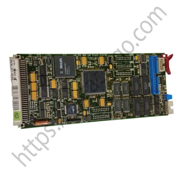
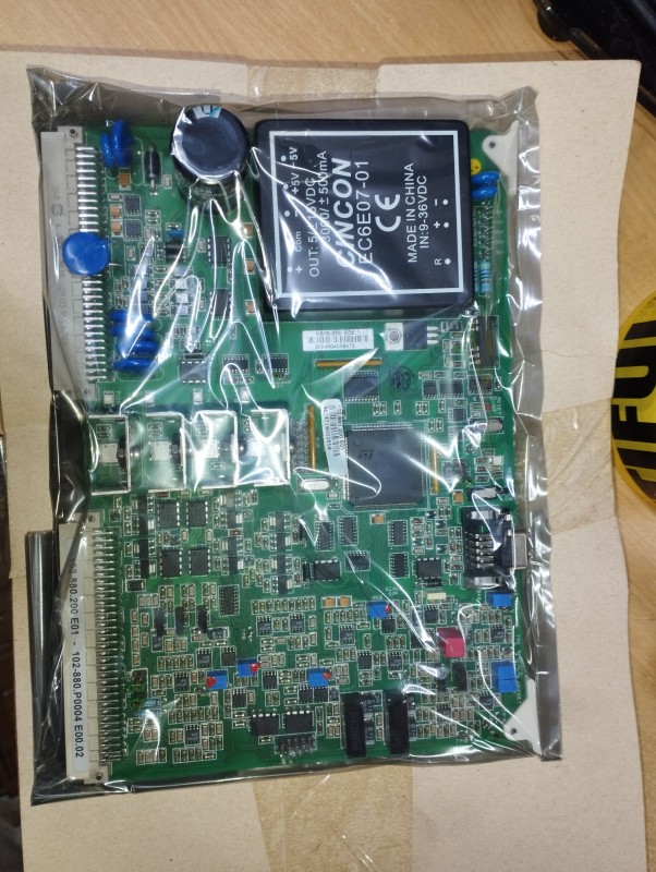
PCB Board Design: The Cornerstone of Modern Electronics
In the rapidly advancing world of
technology, PCB board design plays a critical role in creating the
devices we rely on daily. From smartphones to industrial machines, PCBs
(Printed Circuit Boards) serve as the backbone of electronic circuits, ensuring
seamless communication and functionality between components.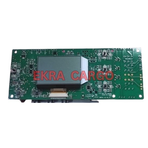
Discover a wide range of PCB-related
tools and resources on Ekra Cargo's PCB search page.
What
is PCB Board Design?
PCB board design involves the intricate process of planning, creating, and
optimizing a printed circuit board. A PCB acts as the framework that houses
electronic components and provides the necessary connections through conductive
pathways. The design process requires precision and expertise to ensure
efficiency, durability, and cost-effectiveness.
For a deeper understanding of PCB
technology, visit the Wikipedia page on Printed Circuit Boards.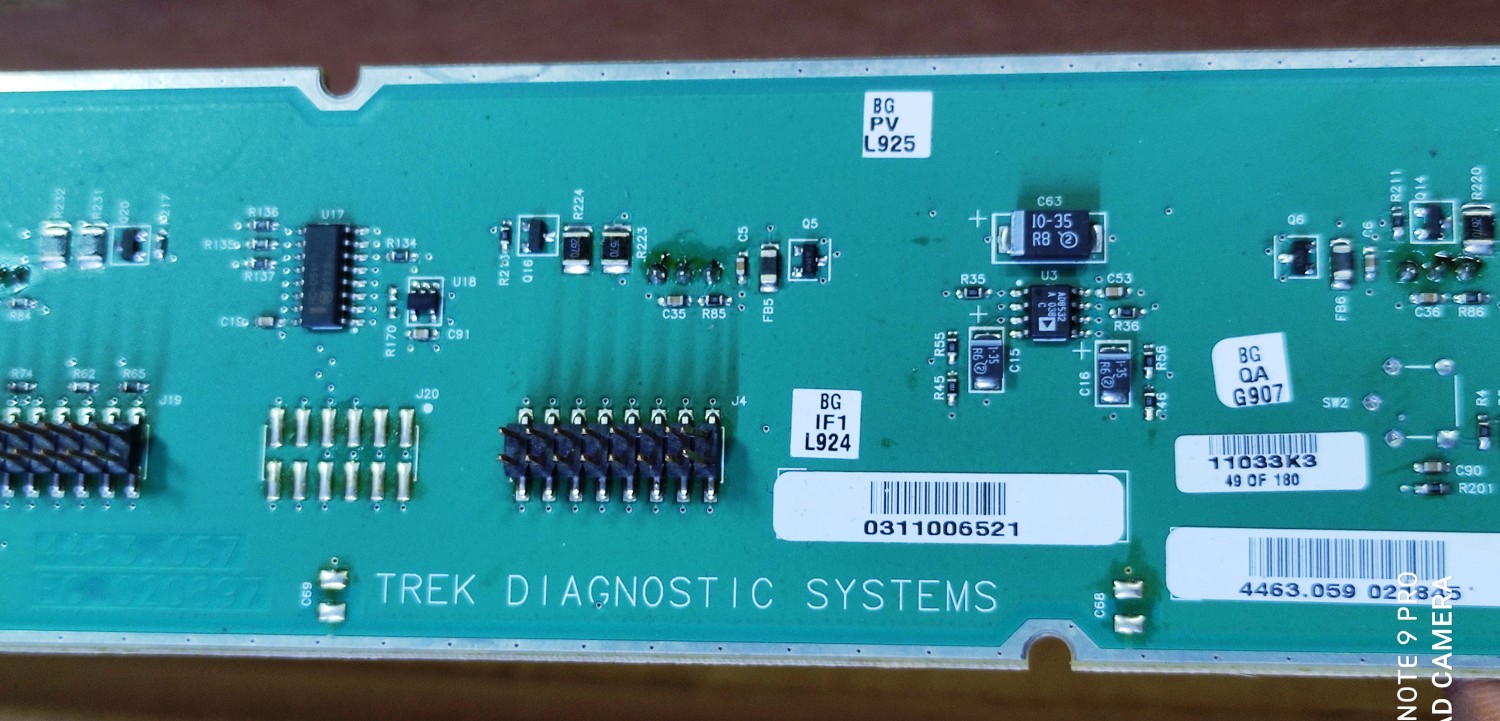
Key
Elements of Effective PCB Design
- Component Placement:
Proper arrangement of components is crucial for functionality and ease of
manufacturing. Ensure components are placed logically to minimize signal
interference and heat issues.
- Layer Organization:
PCBs can be single-layer, double-layer, or multi-layer, depending on
complexity. Multi-layer designs provide more space for connections but
require advanced techniques.
- Signal Integrity:
Maintaining clear and stable signal pathways is essential for
high-performance electronics.
- Thermal Management:
Overheating can damage components. Incorporating heat sinks and
maintaining proper spacing are vital.
Steps
to Create a PCB Board Design
- Define the Circuit Requirements: Understand the purpose and constraints of the design.
- Schematic Design:
Create a detailed schematic using software tools.
- Layout Design:
Use CAD software to design the physical layout, including component
placement and routing.
- Prototyping and Testing: Build a prototype to test functionality and make
necessary adjustments.
- Manufacturing:
Once finalized, the design is sent for mass production.
Explore a wide range of PCB-related
tools and resources on Ekra Cargo's PCB search page.
Why
Choose Expert PCB Design Services?
Professional PCB design ensures your
products meet industry standards while reducing time-to-market. Reliable PCB
designs result in:
- Enhanced performance and reliability
- Cost savings through efficient manufacturing
- Future-proof solutions for scaling and upgrades
The
Future of PCB Design
As technology evolves, so does the
demand for innovative PCB designs. Advanced techniques such as flexible PCBs,
3D printing, and AI-driven design tools are shaping the future of this
essential field. Staying updated with trends is vital for businesses looking to
lead in electronics manufacturing.
By investing in robust PCB board
design practices, industries can build products that meet modern demands while
ensuring efficiency and sustainability.

Ekracargo.com - Your trusted partner in industrial efficiency, providing a wide range of premium quality spare parts at competitive prices.
Contact Info
- Address: House 54 | Road 14 | Sector 14 | Uttara | Dhaka 1230 | Bangladesh
- Phone: Contact: +8801634736139,+8801789394669 (WhatsApp)
- Email: info@ekracargo.com